The applied metallization of an RF device acts as boundary condition that determines the possible electromagnetic field distribution. The electrical properties, the mechanical properties and the geometrical shape have to be considered in this context. These characteristics are related with each other. The condition of the metal layer induces conductor losses that occur in addition to the dielectric losses in the plastic material. The losses are determined by the electric conductivity of the plating material, the geometric dimensions and the geometric surface condition. In case of LDS metallization more than one metal layer is typically applied (typically Cu + ENIG, instead of nickel palladium can be used, an alternative for gold is a silver finish). The resulting conductivity depends on the electromagnetic field distribution occurring on a specific structure. Besides this, the skin effect that defines a frequency related field displacement in electric conductors has to be considered.
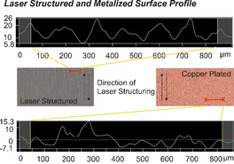
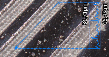
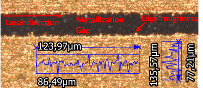
Evaluating the condition of the surface, roughness parameters like the arithmetic mean roughness Ra or Sa and the maximum height Rz or Sz are typically used. The resulting roughness values for the LDS test samples are considerably higher than for typical RF laminates with a rolled copper layer. When evaluating the surface properties of the LDS metallization these higher values defined by Sz and Sa are partially insufficient due to the fact that the exact shape of the surface will additionally influence the losses. In case of the LDS manufacturing the laser causes grooves where the laser beam activated the surfaces to be metallized. This leads to a waviness that depends on the laser beam width, the overlap, the pulse repetition rate and the laser power used for structuring. Fig. 1 depicts one example of a laser structured part where the grooved surface due to the laser is analyzed. A 3D profile view of the structured (bottom) and metallized (top) surface shows the laser induced surface modulation. Fig. 2 shows the dependency of the roughness / waviness of the metallized surface on the laser direction. Another form of roughness aside from surface roughness is edge roughness, as can be seen from Fig. 2 which shows the metallization gap of a coplanar waveguide. This kind of roughness profile has an impact on the characteristic impedance of the waveguide and leads to increased conductor losses and so to increased attenuation, too.


The plating process leads to a slight reduction of the depth of the laser induced grooves. It has to be considered that for an RF application the effective surface is not automatically the outer side of the metallized surface. Depending on the electromagnetic field distribution the inner surface connected to the substrate can also be decisive. The described surface modulation has a high impact on the resulting roughness values while the influences on the RF losses may be lower due to the specific shape of the surface. Therefore, the RF losses are evaluated based on a field simulation where the LDS structured surface is built up as modulated surface with a sinusoidal shape. The detailed description of this investigation and the corresponding results can be found in [1]. These simulations showed that the laser induced grooves on the structured surface do not have the high impact as it may be expected. The induced losses can be influenced by the direction the part is structured. Structuring in line with the wave propagation showed nearly no differences between a smooth and a sinusoidal modulated conductor. For a structuring across the direction of wave propagation the induced losses are increased from 0.91 dB/cm up to 1.09 dB/cm for a coplanar waveguide (CPW) on Xantar LDS 3730 at 50 GHz. To prove the results evaluated by simulation in the next step the insertion loss of a CPW was measured. Different laser inclination angles (α = 0° and α = 45°) are used to structure the test samples that are typical RF transmission lines, metalized with plain LDS electroless copper and galvanic reinforced copper. A detailed description of the measurement setup and measurements for other typical LDS metallization compounds can be found in [1].
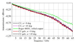


Fig. 3 shows the insertion loss in dB/cm for the evaluated test samples. The laser structuring is done in parallel to the direction of wave propagation with a laser angle of 45 deg and 0 deg. For comparison a CPW fabricated in a photolithographic process with a single layer of rolled copper on Rogers 4003C is measured (black line). At 60 GHz the CPW test samples with copper show a loss of about 0.9 dB/cm while the sample on Rogers 4003 with the rolled copper foil induces a loss of about 0.75 dB/cm. The conductivity of LDS copper is only about 30 MS/m while the conductivity of the rolled copper can be assumed to be above this value. Furthermore, the LDS substrate material used (Xantar LDS 3730) has a loss tangent of about DF = 0.006 at 20 GHz. The Rogers 4003C laminate provides a loss tangent of about DF = 0.0027 at 10 GHz. Consequently, the higher losses that can be observed for the LDS manufactured samples may not only be due to conductor losses, but also due to the dielectric losses. These aspects prove the assumption that the surface roughness values of LDS copper do not have the high impact on the losses as it may be expected. This can be explained by the specific shape of the laser structured surfaces with their laser induced grooves leading to a kind of surface modulation that only slightly influences the conductor losses. With regard to the manufacturing process the evaluations indicate that even though that there are only slight differences a structuring in parallel to the direction of the electromagnetic wave propagation is recommended.
References
[1] A. Friedrich, M. Fengler, B. Geck (2016): LDS MIDs Fit for mmWave, Microwave Journal, no. 9, vol. 59, September 2016
[2] A. Friedrich, M. Fengler, B. Geck (2016): LDS Manufacturing Technology for Next Generation Radio Frequency and Sensor Applications - A discussion on Requirements and Solutions -, 12th International Congress Molded Interconnect Devices 2016, Würzburg, Germany, September 28-29, 2016
[3] Q. H. Dao, A. Friedrich, B. Geck (2014): Characterization of Electromagnetic Properties of MID Materials for High Frequency Applications up to 67 GHz, 11th International Congress Molded Interconnect Devices 2014, Nuremberg/Fuerth, Germany, September 24-25, 2014
[4] A. Friedrich, Q. H. Dao, B. Geck (2014): Charakterisierung der Hochfrequenz-Eigenschaften von Materialien für LDS-MID, PLUS Produktion von Leiterplatten und Systemen, Leuze Verlag, Februar, 2014

